A Software for Simulating Dispersive Properties of Multilayered Phononic Crystal Membranes
Master’s Thesis in Physics
18.10.2021
Jyväskylän yliopisto, Matemaattis-luonnontieteellinen tiedekunta, Fysiikan laitos
University of Jyväskylä, Faculty of Mathematics and Science, Department of Physics
Author: Panu Lappalainen
Instructor: Tuomas Puurtinen
Page count: 73
Työn otsikko: Ohjelmisto monikerroksisten fononikidekalvojen dispersiivisten ominaisuuksien simulointiin
Published at: http://urn.fi/URN:NBN:fi:jyu-202111195725
Tässä tutkielmassa kehitetty uudenlainen Kalvo-ohjelmisto simuloi monikerroksisten sylinterireikähilaisten fononikidekalvojen dispersioita äärelliselementtimenetelmää (FEM) käyttäen. Havainnollistavan systemaattisen fononikidetutkimuksen simulaatioissa käytettiin neljää erilaista laboratoriossa usein käytettyä materiaalia: piinitridiä (Si3N4), alumiinioksidia (Al2O3), polystyreeniä (PS) ja lyijyä (Pb). Vastaavan laajuista systemaattista tutkimusta ei ole aiemmin kyetty tekemään.
Aiemmista simulaatioista tunnetaan, että sylinterireikäisellä Si3N4-fononikiteellä, jonka täyttöaste  , hilavakio
  ja kalvonpaksuus
 , on spektriaukko, jonka suhteellinen koko
  . Osoittautui, että tätä spektriaukkoa on mahdollista laajentaa lisäämällä kalvoon kerros toista materiaalia. Ohjelmistoa käyttäen löydettiin uusi rakenne, jolla hilan spektriaukon suhteelliseksi kooksi saatiin simuloitua
  (kun ) käyttäen Si3N4–Al2O3-kaksikerroskalvoa, jonka
  ja
ja  . Tällä materiaalikonfiguraatiolla on spektriaukko vain kun
  . Tämä spektriaukko laajenee nopeasti täyttöastetta kasvatettaessa, kunnes
  , minkä jälkeen aukon laajanemistahti hidastuu merkittävästi. Si3N4-kalvon spektriaukkoa ei saatu laajennettua polystyreeni- tai lyijykerroksilla. Fononikiteen dispersiorelaatiot muuttuvat, jos toinen kaksikerroskalvon materiaaleista jaetaan kahtia ympäröimään toista materiaalia, eritoten jos jaettava materiaali on jäykempi kahdesta. Esimerkiksi Si3N4–PS- ja PS–Si3N4–PS-kalvoilla on spektriaukko, kun
  ja , mutta vastaavalla Si3N4–PS–Si3N4-kalvolla ei.
Ohjelmisto osoittautui hyödylliseksi monikerroksisten fononikiteiden dispersiorelaatioiden systemaattiseen tutkimukseen.
Avainsanat: fononikide, dispersio, monikerroskalvo, simulaatio-ohjelma, FEM, piinitridi
This thesis introduces Kalvo, a new type of software developed for simulating the dispersions of multilayered phononic crystal membranes with a cylindrical hole lattice, using the finite element method (FEM). The simulations in a demonstrative systematic study used four different materials commonly used in laboratory: silicon nitride (Si3N4), aluminum oxide (Al2O3), polystyrene (PS) and lead (PS). A systematic study of this scale has not been possible before.
It is known from prior simulations that a Si3N4 phononic crystal with cylindrical hole lattice, filling factor , lattice constant and Si3N4 membrane thickness  , has a relative band gap . Using the software, it was found out that this band gap could be increased to (for ), by using a Si3N4–Al2O3 dual layer membrane with and . For this configuration of materials, the band gap exists only when . This band gap widens rapidly as filling factor is increased, until , after which the rate of increasing decreases significantly. The Si3N4 membrane’s band gap could not be widened with layers of polystyrene or lead. The band structure of a phononic crystal is changed if one of the materials in a dual layer membrane is distributed into two layers surrounding the other material, especially if the stiffer of the two materials is distributed. For instance, a band gap exists for a Si3N4–PS and PS–Si3N4–PS membranes with
  to
to  ratio of
  and , but not for Si3N4–PS–Si3N4.
The software proved to be useful for systematically studying the band structures of multilayered phononic crystals.
Keywords: phononic crystal, dispersion, multilayered membrane, simulation software, FEM, silicon nitride
Acknowledgements
This is the electronic version of this thesis with features such as interactive animated components. These are utilized in this work, since many of the diagrams have more than two variables, which cannot realistically be visualized with 2D plots, nor clearly in 3D plots. Subtle differences are difficult to see even in a side-by-side comparison and are best visualized with animations, where a third variable can be represented by time (or user action). Due to current technological limitations in printing moving images on paper, the animated components are replaced by side-by-side image montages in the PDF version of this document. (Please use the PDF version for printing.)
Two years ago I fell asleep during a nanoseminar course and only I woke up to the closing words of Dr. Tuomas Puurtinen about him needing someone with studies in physics and information technology for his project. Not knowing what I was signing up for, but identifying with these requirements, I approached him and got pulled into this project in professor Ilari Maasilta’s thermal nanophysics research group. During the work on this project I have learned about meshing, scripting, computing and programming in five different languages, in addition to acquiring many other interesting skills. I wish to thank Dr. Puurtinen for his guidance throughout this project.
Table of Contents
See “Document index” (opened by the book icon on the upper left-hand corner).
1. Introduction
Heat is nice. On a cold winter day, one may spend a lot of firewood or electricity to heat up a sauna, often to very high temperatures, in order to enjoy the hot steam. However, too much heat in the wrong place can be problematic. For instance, it is a good idea to isolate the heat from getting into other rooms, such as the bedroom, in order to guarantee a good night’s sleep.
Condensed matter physics is a field of natural sciences that studies the microscopic and macroscopic physical properties of matter, especially solids and liquids. One of the properties studied is thermal conductivity, a material’s ability to conduct heat. Materials with high thermal conductivity are called conductors, whilst those with low thermal conductivity are called insulators. Different materials are desirable for different applications, and sometimes conduction or insulation is only required for a certain range of frequencies.
It is possible to design and develop materials with very specific properties. However, obtaining the materials and fabricating the structures, especially in nano scale, can be rather expensive and time consuming. Hence, finding suitable material configurations by means of trial and error is experimentally unpractical. On the other hand, the chaotic nature of the phonon dispersions makes purely theoretical approach difficult. (Some partial differential equations can be impossible to solve analytically, thus only approximate numerical solutions can be found for them.) The software introduced in this thesis can be used to computationally find, simulate and study such crystal membrane structures systematically before physically fabricating them.
1.1 Metamaterials
Not all materials are created equal. Despite two materials sharing the same chemical formula, their physical properties can still vary. This can be explained with differences in their crystalline structure. These varieties of material are called allotropes, and many examples exist in nature. Diamond and graphite, for instance, both consist of pure carbon, yet diamond is much harder with higher thermal conductivity and lower electrical conductivity than graphite. [Royer-Dieulesaint-2000]
Metamaterials (from Greek, “beyond matter”) are materials engineered to have benefits beyond those of naturally occurring materials. They are usually precision manufactured to contain repeating patters that can be at a scale smaller than the wavelength of the phenomenon they influence, such as sound or electromagnetic waves. Metamaterials can have peculiar properties, e.g. negative refraction, superlensing or even programmability. [Cui-2014]
The history of metamaterials can be traced all the way back to the 19th century, beginning around 1888 with Heinrich Hertz demonstrating the interactions of metals and radio waves, eventually leading to the artificial dielectrics, a type of fabricated composite materials. The first “metamaterials” were designed after the Second World War, to interact with radio and microwave frequencies in the early antenna and waveguide technologies. [Ramsay-1958]
1.2 Crystals and Acoustic Metamaterials
Crystal lattices have their constituents arranged in a highly ordered microscopic structure. Phonons are collective excitations of the constituents in crystals and in other condensed matter with periodic and elastic arrangements of constituents. Thermal phonons, among other factors, are responsible for conduction of heat in crystals. The behaviour of these phonons is highly dependent on the crystal structure of the lattice. Artificial crystals, the topic of interest in this work, differ from natural crystals in being made by technology or craft. [Kittel-1996, Laude-2020]
Phononic crystals, often PnCs for short (not to be confused with PCs, photonic crystals), are designed to manipulate sound waves or phonons in a desired way. For instance, thermal properties of a material are affected by the conductivity for different frequencies of phonon waves. This is often plotted in a band structure dispersion spectrum of the lattice. Since crystals have a highly ordered structure, their thermal behaviour can be very accurately simulated computationally by calculating the dispersions of the phonons. The dispersion frequencies are obtained by applying Bloch’s theorem on a unit cell in the reciprocal lattice space. The unit cell is a repeating unit that can be used to describe the crystal structure of a material. Producing approximations for the frequencies involves solving partial differential equations in three space variables. [Li-Wen-Sheng-2021]
One application of these materials is acoustic cloaking, which aims to make an object “invisible” to sound waves by covering it with anisotropically elastic materials. This can be done with a coordinate transformation method, but a viable cloak requires the optimal topology and materials with extreme properties. In 2017, Méndez et al. used a topological derivative and the level set function based topology optimization technique to design and synthesize such a device, noting the key significance of the external shape of the prescribed domain of the optimization. Acoustic cloaking has potential uses in stealth technology and in concert hall or household sound proofing solutions. [Mendez-2017]
1.3 Heat in Low Temperature Regime
In extremely low temperatures, the impact of thermal fluctuations is amplified. Phononic crystals, especially ones with large band gaps in the band structure, have many useful applications here. (Moreover, the size of the band gap width-to-midpoint ratio matters, as the band structure can be scaled!) The thermal phonons with long wavelengths mainly populate in low temperatures; when the surface features of the medium are small compared to the phonon wavelength, the phonons can be treated as ballistic waves whose propagation and speed can be manipulated. Phononic crystals fabricated in a suspended membrane can significantly reduce the thermal conductance in sub-Kelvin temperatures.
Low temperature detectors, such as microwave kinetic inductance detectors (MKIDs), have been shown to benefit from nanoscale phononic crystals tailored for them. MKIDs are extremely sensitive non-bolometric photon detectors, which work by creating quasiparticles via the incident photons breaking Cooper pairs. However, the quasiparticles quickly recombine back into Cooper pairs, and the emitted photons escaping the system limit the responsivity of the detector. In 2020, Puurtinen et al. demonstrated that a composite phononic crystal reached a power attenuation of  , effectively increasing the quasiparticle lifetime by two orders of magnitude. [Puurtinen-2020]
In the low-temperature phononic crystal studies in the Nanoscience Center at the University of Jyväskylä, a phononic crystal is “built” around the sample, by fabricating and etching a phononic crystal structure around superconductor–insulator–normal metal–insulator–superconductor tunnel junction (SINIS), in the same membrane. The etching can be performed with electron beam lithography. These phononic crystal structures have been demonstrated to have smaller conductivity than the membrane, mainly due to the band structure and the presence of certain band gaps. [Tian-2016]
1.4 Motivation
It should be noted that even though theoretical structures can have unfathomable properties that natural materials lack, they can be practically impossible to manufacture. Developing a realistically viable phononic crystal with specific desired properties requires simulating multiple configurations of structures with real material parameters, all whilst taking into account the limitations in fabrication. [Lucklum-Vellekoop-2017]
Thus, the aim of this work is
- to develop a lightweight, user-friendly software that can be used for fast systematic analysis of phononic crystal membranes, and
- to demonstrate the software by using it to increase the band gap of a known phononic crystal through a systematic study involving realistic materials.
The numerical method used in this thesis is the finite element method (FEM), which solves the problem by subdividing the system into smaller parts. In the software created in this work, a mesh of the unit cell is created using hexahedral elements. (Hexahedron is a six-faced polyhedron, e.g. a cube.) The mesh is constructed and solved using the Lawrence Livermore National Laboratory C++ library MFEM and associated tools. [Zienkiewicz-2013, Anderson-2021, Kolev-Dobrev-2010]
The software introduced in this work, Kalvo (Finnish for “membrane”), is specifically tailored to solve the dispersions of a single- or multilayered phononic crystal membrane. A systematic study of multilayered phononic crystals has not been done before and few other tools exist that could be used for this task. The commercial COMSOL Multiphysics® is one of the tools often used in computational studies, one such by Jia et al. in 2018, to design phononic crystals with wide band gaps. However, (unlike with COMSOL Multiphysics®) with the Kalvo software the 3D mesh does not need to be modelled by the user, but is instead generated automatically from the given parameters. This is one of many advantages of this software as it can be run entirely with a command prompt and is thus Bash-scriptable, opening avenues for quickly checking the dispersions of different structures on a cluster computer. [Comsol-2020, Jia-2018]
2. Theory
2.1 Applying Bloch’s Theorem
For a crystal lattice, according to the Bloch’s Theorem, a periodic function  with the same periodicity as the crystal modulates the plane wave
  describing the Schrödinger equation of the lattice,
  = u(\mathbf{r}) e^{\iota\mathbf{k \cdot r}}
\end{equation}") where
where  is the position,
  the wave vector and
  the imaginary unit. [Ibach-Luth-2009]
In a membrane that is periodic in the two horizontal dimensions,  and
and  , this means that for a unit cell,
 })
\end{equation}") where
where  is the boundary opposite to
  and
and  and
and  are the wave vector components in the - and -direction, respectively. Therefore, by labelling the horizontal boundaries of the unit cell clockwise from 1 to 4,
 })
\text{, \: \:}
u \Big|_{B_2} = u \Big|_{B_4} \exp({\iota(k_x x + k_y y)}).
\end{equation}")
2.2 Linear Elasticity of Crystals
Derived from the mechanical equilibrium, Hooke’s law and Cauchy’s strain tensor, for isotropic and homogeneous materials, the Navier–Cauchy equation can be applied,  \nabla (\nabla \cdot \mathbf{u})
= \rho \frac{\partial^2 \mathbf{u}}{\partial t^2},
\; \text{\scriptsize{(Eq. NC1)}}
\end{equation}")
where  is the material density and
  and
and  are Lamé parameters derived from Young’s modulus
  and Poisson’s ratio
  such that
 (1-2\nu)},\\
\mu &= \frac{E} {2(1+\nu)}
\end{aligned}
\; \text{\scriptsize{(Eq. NC2)}}
\end{equation}") and
and ") is the displacement vector with components
is the displacement vector with components )") where
where  . [Palermo-Marzani-2020, Li-Wen-Sheng-2021]
Thus, assuming a solution  with components
 ") , substitution into Equation NC1 yields the constant
, substitution into Equation NC1 yields the constant  from the exponent and the exponent term can be divided out. Therefore the components of Equation NC1 can be presented as
+(\lambda + \mu)
\frac{\partial(u_{11}+u_{22}+u_{33})}{\partial x}
= -\rho \omega^2 u_1 \\
\mu \left(\frac{\partial u_{21}}{\partial x}
+\frac{\partial u_{22}}{\partial y}
+\frac{\partial u_{23}}{\partial z} \right)
+(\lambda + \mu)
\frac{\partial(u_{11}+u_{22}+u_{33})}{\partial y}
= -\rho \omega^2 u_2 \\
\mu \left(\frac{\partial u_{31}}{\partial x}
+\frac{\partial u_{32}}{\partial y}
+\frac{\partial u_{33}}{\partial z} \right)
+(\lambda + \mu)
\frac{\partial(u_{11}+u_{22}+u_{33})}{\partial z}
= -\rho \omega^2 u_3
\end{aligned}
\end{equation}") where
where  This is known as the strong form.
Solving this system numerically with FEM requires the equation to be transformed into the weak form. This transformation can be performed by first multiplying each component by a test function  , integrating over the solution domain
  and moving one of the derivation operations in each term onto the test functions using Green’s first identity. [Laude-2020, Strauss-2007]
  \\
&-\lambda\left(\frac{\partial v^*_1}{\partial x}\frac{\partial u_1}{\partial x} +
\frac{\partial v^*_1}{\partial x}\frac{\partial u_2}{\partial y} + \frac{\partial
v^*_1}{\partial z}\frac{\partial u_3}{\partial x}\right) \\ &-\mu\left(\frac{\partial
v^*_1}{\partial x}\frac{\partial u_1}{\partial x} + \frac{\partial v^*_1}{\partial
y}\frac{\partial u_2}{\partial x} + \frac{\partial v^*_1}{\partial x}\frac{\partial
u_3}{\partial z}\right)\Bigg) = \int_\Omega-\rho \omega^2 v^*_1u_1 \\
\int_\Omega\Bigg( &-\mu \left(\frac{\partial v^*_2}{\partial x}\frac{\partial
u_2}{\partial x} + \frac{\partial v^*_2}{\partial y}\frac{\partial u_2}{\partial y} +
\frac{\partial v^*_2}{\partial z}\frac{\partial u_2}{\partial z}\right)\\ &
-\lambda\left(\frac{\partial v^*_2}{\partial x}\frac{\partial u_1}{\partial y} +
\frac{\partial v^*_2}{\partial y}\frac{\partial u_2}{\partial y} + \frac{\partial
v^*_2}{\partial z}\frac{\partial u_3}{\partial y}\right)\\ & -\mu\left(\frac{\partial
v^*_2}{\partial y}\frac{\partial u_1}{\partial x} + \frac{\partial v^*_2}{\partial
y}\frac{\partial u_2}{\partial y} + \frac{\partial v^*_2}{\partial y}\frac{\partial
u_3}{\partial z}\right)\Bigg) = \int_\Omega-\rho \omega^2 v^*_2u_2 \\
\int_\Omega\Bigg( &-\mu \left(\frac{\partial v^*_3}{\partial x}\frac{\partial
u_3}{\partial x} + \frac{\partial v^*_3}{\partial y}\frac{\partial u_3}{\partial y} +
\frac{\partial v^*_3}{\partial z}\frac{\partial u_3}{\partial z}\right)\\ &
-\lambda\left(\frac{\partial v^*_3}{\partial x}\frac{\partial u_1}{\partial z} +
\frac{\partial v^*_3}{\partial y}\frac{\partial u_2}{\partial x} + \frac{\partial
v^*_3}{\partial z}\frac{\partial u_3}{\partial z}\right)\\ & -\mu\left(\frac{\partial
v^*_3}{\partial z}\frac{\partial u_1}{\partial x} + \frac{\partial v^*_3}{\partial
z}\frac{\partial u_2}{\partial y} + \frac{\partial v^*_3}{\partial z}\frac{\partial
u_3}{\partial z}\right)\Bigg) = \int_\Omega-\rho \omega^2 v^*_3u_3 \end{aligned}
\; \text{\scriptsize{(Eq. NC3)}}
\end{equation}")
Since this form of the equation lacks the time-dependent term, using the Floquet-Bloch Theorem, solutions for this system can be found in the form \,U_i,
\end{equation}") where
where ") is the wave vector,
is the wave vector,  are periodic functions in and
 ") . It can also be assumed that the test function is of the same form,
. It can also be assumed that the test function is of the same form, \, V_i,
\end{equation}") where the exponential term has a positive sign, due to complex conjugation. This will cause the exponential factors to cancel out at the end. [Garcia-Alvarez-2015]
where the exponential term has a positive sign, due to complex conjugation. This will cause the exponential factors to cancel out at the end. [Garcia-Alvarez-2015]
The derivatives for  and can be calculated and substituted into Equation NC3. In the left-hand side of the first component, for the terms with no derivatives this is
  + k_y^2\mu) V_1U_1 + k_xk_y(\lambda + \mu) V_1U_2
\big), \\ \end{aligned} \; \text{\scriptsize{(Eq. W0)}}
\end{equation}") for the imaginary terms with one derivative
for the imaginary terms with one derivative  \frac{\partial V_1}{\partial x}U_1
&-k_x(\lambda + 2\mu) \frac{\partial U_1}{\partial x}V_1\\
+k_y\mu\frac{\partial V_1}{\partial y}U_1 &-k_y\mu \frac{\partial
U_1}{\partial y} V_1\\
+k_y\lambda \frac{\partial V_1}{\partial x} U_2 &-k_y\mu \frac{\partial
U_2}{\partial x}V_1\\
+k_x\mu \frac{\partial V_1}{\partial y}U_2 &-k_x\lambda \frac{\partial
U_2}{\partial y}V_1\\
+k_x\mu \frac{\partial V_1}{\partial z}U_3 &-k_x\lambda \frac{\partial
U_3}{\partial z}V_1 \bigg) \iota \end{aligned} \; \text{\scriptsize{(Eq. W1)}}
\end{equation}") and for the second derivative terms (the “Navier-Cauchy terms” for the Bloch wave coefficient functions )
and for the second derivative terms (the “Navier-Cauchy terms” for the Bloch wave coefficient functions ) \\
+\lambda\bigg(\frac{\partial V_1}{\partial x}\frac{\partial U_1}{\partial x}
&+ \frac{\partial V_1}{\partial x}\frac{\partial U_2}{\partial y}
+ \frac{\partial V_1}{\partial z}\frac{\partial U_3}{\partial x}\bigg)\\
+\mu\bigg(\frac{\partial V_1}{\partial x}\frac{\partial U_1}{\partial x}
&+ \frac{\partial V_1}{\partial y}\frac{\partial U_2}{\partial x}
+ \frac{\partial V_1}{\partial x}\frac{\partial U_3}{\partial z}\bigg)\Bigg).
\end{aligned} \; \text{\scriptsize{(Eq. W2)}}
\end{equation}")
2.3 Generalized Eigenvalue Problem
The linearization of the weak form can be done by using e.g. the variational method or the Galerkin method. In this work, the linearization of the weak form is performed internally, using the built-in classes and methods of the MFEM library, which uses the variational method. The exhaustive process of transforming the weak form into matrix form with methods including the Galerkin method is explained well in the literature of the Polish-British FEM pioneer Olgierd Zienkiewicz. [Zienkiewicz-1977, Zienkiewicz-2013]
As a brief summary of the variational method, the solution domain is discretized into a finite mesh  and the linear combination of basis functions is substituted into the weak form. The basis functions are also selected as the test functions. In order to obtain a linear system, using the linearity of the summation, the weak form is manipulated such that the integration applies to the basis functions and their derivatives. As the basis functions and their derivatives are known, their integrals can be computed, thus only a linear system of equations remains. Now, two square matrices are defined from this system,
  (stiffness) and
  (mass), which are functions of , and the material parameters. [Zienkiewicz-Morgan-1983]
Hence, the eigenfrequencies for the band structure of the material can be computed from the obtained generalized eigenvalue problem }}
\end{equation}") where
where  is the eigenvector and is a scalar known as the eigenvalue, the root of the characteristic polynomial. Since
  is the eigenfrequency of the phonon, by solving the eigenproblem for a range of values in
  -space, the band structure can be plotted. [Laude-2020]
2.4 Phonon Dispersion
The natural modes of periodic media are known as Bloch waves. Their propagation rate  is called the phase velocity, and the propagation velocity of the overall envelope of their amplitudes
  is called the group velocity, required for thermal conductivity calculations. Their dispersion properties can be presented with band structure diagrams, which plot these eigenmodes with reference to the first Brillouin zone of the medium. For thin crystal membranes, the waves in the two horizontal dimensions are usually studied. Since plotting the dispersion behaviour in all of -space would yield a three-dimensional diagram (which is sometimes used) the dispersions are often plotted along a path through the irreducible Brillouin zone (IBZ), shown in Figure D1. [Laude-2020]
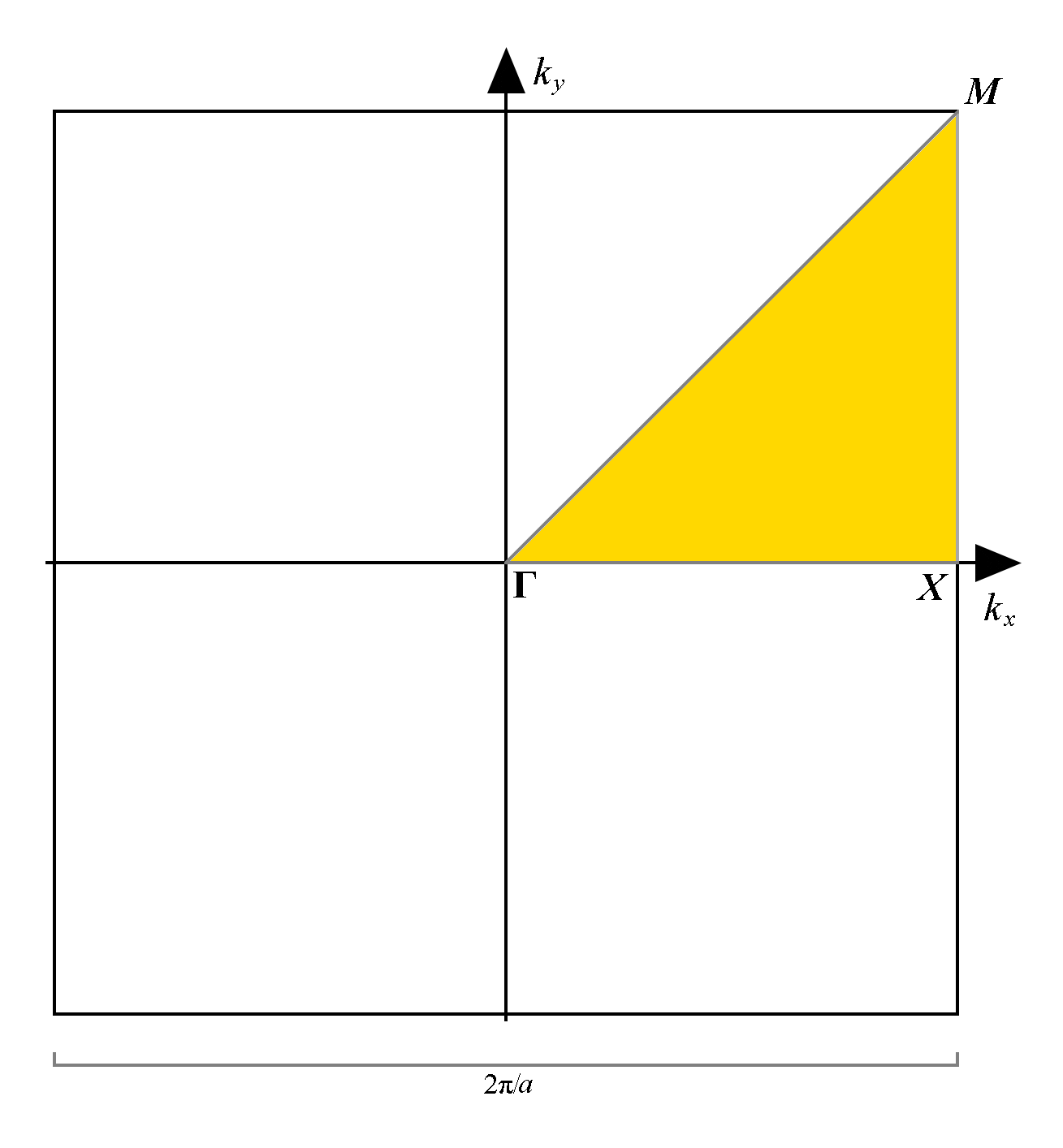
 . Here, for a membrane with rotational and reflection symmetry of order 4, the irreducible Brillouin zone is highlighted in yellow, with a grey path connecting the corner points of the IBZ triangle labelled as
  ,
,  and .
and .In thin membranes, the phonons traversing along the “planar” dimensions ( and ) of the geometry are the topic of study in this work. Hence, the main symmetry points of interest are:
- (“Gamma”), the center of the Brillouin zone;
- , the center of a face;
- , the center of an edge.
For membranes with rotational and reflection symmetry of order 4, these three symmetry points are sufficient. For full membranes (as there are infinite symmetry axes), the behaviour is the same regardless of direction, requiring only two points. This is clearly demonstrated in the band structure depicted in Figure D2, where the -axis comprises of the path from to , then to and finally back to . Notice that since the reduced Brillouin zone selected is a right-angled isosceles triangle in this case, the – section of the path is  times as long as the – and - sections.

 of Si3N4 and
  of Al2O3. (Here, the symmetry points and are indicated with gray vertical bars, for clarity.) Because the material is a full membrane, the modes between points – also appear between points – (but as larger and in reverse order).
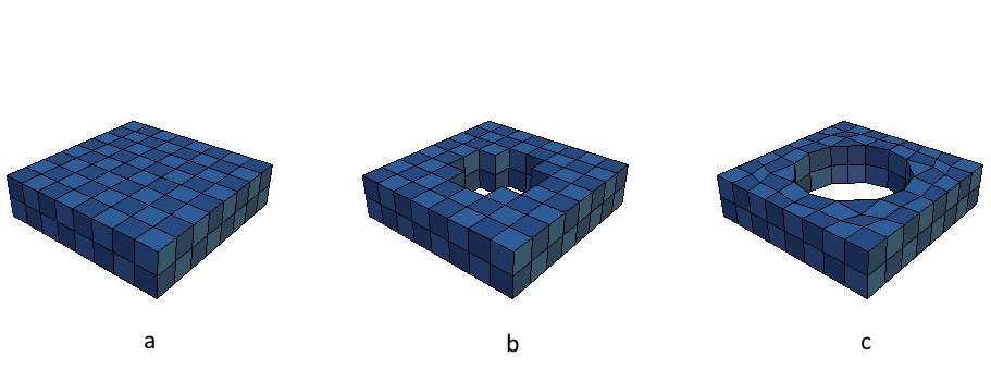
Band gaps occur when there are no propagating Bloch waves for a certain frequency range, regardless of wave number (as seen in Figure D3 in the red area clear of any modes). In these gaps, no propagation is possible for the range of frequencies in any direction. Band gaps have endless potential practical applications, providing useful functionalities in e.g. mirrors, cavities, and waveguides. Membranes with band gaps occurring in the band structure can be created with e.g. periodic hole and pillar structures. Computationally studying band gaps formed by cylindrical holes in square grid is the main focus of this work. [Laude-2020]
Whilst studying band structures, an important thing to note is the linear scalability. Since the periodicity of artificial crystals is significantly greater than interatomic distances (unlike in natural crystals), macroscopical analysis using the equations of continuum mechanics can be performed for them. Although the results in this work are mainly presented in the absolute units the simulations were performed in, they can easily be scaled to desired frequencies by inversely scaling all of the parameters. Figure D3 demonstrates how the frequencies of the entire band structure are scaled down to half when all of the parameters are scaled up to double.
 and
and  of
of  and , lattice constant of
  and a cylindrical hole with radius
  of
of  (left), compared to same lattice with all parameters doubled (right), demonstrating the same band structures in different scales. To aid comparison by eye, the -axis scale of the right diagram is half of that of the left one, and a band gap is highlighted in red.
The precision of the band structure is determined by the -space sampling resolution, i.e. how many points in the -space are computed for the plot. The number of eigenfrequencies computed roughly translates to the number of modes in the plot. For most eigenvalue solvers however (including the SLEPc used in this work), the order the eigenvalues are computed in is inconsistent with the order of the modes. Thus, in this work the obtained eigenfrequencies are sorted by frequency before plotting. [Roman-2021]
Due to this, connecting the sorted data points with lines will never yield intersecting lines in the plot. Since the real modes overlap and cross over one another, the curves in the band structure cannot be singled out to represent a mode fully through the path over the IBZ. This is clearly visible in Figure D3, where approaching curves appear to “turn away” before ever intersecting; it uses the sampling resolution of 60, thus there are 61 frequency points per mode in the diagram (the values at on the right side are copied from the values at on the left side). Increasing the sampling resolution causes this type of visual artifacts to diminish (for reference, Figure D2 has a sampling resolution of 1000). However, the computation time is directly proportional to the sampling resolution.
Figure D4 demonstrates selecting a number of points in the IBZ path and the band structure they can be used to produce. Using only this few points (7) is unreliable for studying the shapes of the modes. However, it may have applications in searching band gaps, since the local maxima and minima of individual modes are often located at the corner points of the IBZ triangle.
 , to produce the band structure (right) for a silicon nitride phononic crystal with lattice constant of , thickness
  of and filling factor
  of
of  . With a sampling resolution this low, the lines connecting the points do not accurately represent the modes. For comparison, see Figure R1, which plots the same band structure with a sampling resolution of 60.
Band gaps can be computationally found by sorting all computed eigenfrequencies by frequency (for all of the computed points in -space) and looking for big separations between the values. The separation can be calculated by taking the absolute value of the difference between the  th value and the
 ") th value. Should the separation be greater than the acceptable minimum gap size, it can be counted as a band gap. (A Python implementation of this is demonstrated in Appendix 2.)
th value. Should the separation be greater than the acceptable minimum gap size, it can be counted as a band gap. (A Python implementation of this is demonstrated in Appendix 2.)
The acceptable minimum gap size has to be selected carefully; a value too large will neglect real band gaps, but a value too small will produce false positives. A large sampling resolution will diminish this issue and allow using a small minimum gap size. For the majority of the plots in this work, a -space sampling resolution of 60 and an acceptable minimum gap size of  were used.
If a low sampling resolution is used, one way to get rid of false positives due to small acceptable minimum gap size is to add intermediate points between the data points via linear interpolation. These additional points lie on the lines connecting the data points and thus do not disturb the band structure diagram. Performing this does not increase the precision of the plot, but requires significantly less computation power than using a higher sampling resolution. However, this method was not used in this work as the aforementioned parameters were mostly sufficient.
3. Software
3.1 Code
The source code of the Kalvo software is written in C++ programming language with supplementary programs written in Bash and Python. It utilizes Open MPI message passing interface for parallelization and the finite element discretization library MFEM (version 4.1 or higher) together with algorithms of PETSc (“Portable, Extensible Toolkit for Scientific Computation”, version 3.13.3 or higher) and its extension SLEPc (“Scalable Library for Eigenvalue Problem Computations”, version 3.13.3 or higher) for solving the eigenvalue problem from the partial differential equations. Some MFEM integrator inspired integrators were coded specifically for forming the matrices to solve this very eigenvalue problem, with METIS and hypre libraries utilized in the matrices. The software should be compiled with the included makefile, which utilizes mpicxx compiler wrapper (version 4.0.3 or higher) expecting a gcc module of version 10.1.0 or higher. [Balay-2021, Gabriel-2004, Kolev-Dobrev-2010, Roman-2021, Karypis-Kumar-1999, Falgout-Yang-2002]
The software also includes an installation guide and some parameter files. Below is a comprehensible list of included files created for this software.
makefile            Kalvo.cpp
cleeps.cpp          cleeps.hpp
coolPrint.cpp       coolPrint.hpp
material.cpp        material.hpp
meshFactory.cpp     meshFactory.hpp
settings.cpp        settings.hpp
defaultSettings.txt install_guide.txt
k_points.txt        materialParameters.txt
The code uses standard C++ conventions and documentation style. Additionally, in order to further aid future development, the code is heavily commented. Due to the complex nature of creating the 3D geometry, some of the console output and comment documentation utilizes ASCII visualization for added comprehensibility. For example, the hexahedral elements in MFEM are constructed from the nodes (or the vertices) in different order depending on context. Thus, in the MeshFactory::solveHexahedrons subroutine for instance, the construction order is visualized in the comments followingly:
    // Construct the      7-----6
    // hexahedron with   /|    /|
    // vertices from    4-----5 |
    // bottom to top    | 3---|-2
    // anti-clockwise   |/    |/
    // in this order    0-----1
The software is used to solve the eigenfrequencies of a full membrane or a membrane with a lattice of cylindrical holes in a rectangular grid. The membrane can consist of one or more layers of materials. No other types of geometries can currently be created using the software. However, by modifying the source code, support for other geometry types, e.g. pillars, can be added with reasonably little work. The updated code can be found at the project’s GitLab repository. [Lappalainen-Puurtinen-2021]
3.2 Parameters
Upon running the program, several parameters can be given either in the command prompt or in the default settings file. The default settings file parameters are used for parameters not given in the command prompt; those given in the command prompt override their default parameters. For each command prompt parameter of Kalvo, the input string is always a single, case sensitive character, followed by an equals sign (=) and the value. The value parameters containing multiple values should have the values separated by a comma (,). Spaces are used to separate different parameter strings. For instance, the parallel prompt could be
mpirun -n 8 Kalvo a=200 h=50 r=65 m=Si3N4 e=8,,2 k=GXMG,50where the mpirun command launches the job Kalvo in Open Run-Time Environment (ORTE) with -n 8 setting the number of parallel processes as 8. The remaining Kalvo parameters are explained in the subsections below.
3.2.1 Unit Cell Parameters
Three parameters directly affect the geometry of mesh: a, h and r (as demonstrated by Figure M1). All of their values are in nanometers. The lattice constant a determines the widths of the horizontal sides of the rectangular base of the unit cell. If a is given two values, the values represent the width and breadth of two horizontal sides (in - and -dimension). If a is given a single value, the base of the unit cell is a square. (Only square base unit cells are in the scope of the study in this thesis.)
Each value of the thickness h represents the vertical height ( -dimension) of a single material layer in the membrane, with their sum being the total thickness of the unit cell. The number and order of values for
 h must correspond to the number and order of materials in the lattice (parameter m).
The size of a cylindrical hole piercing through the normal of the lattice is controlled with radius parameter r. When r=0, no hole is made (producing a full membrane). It should be noted that the value of r must be less than half of the smallest value of a, since the hole should not be larger than a single cell.
Alternatively, the filling factor F can be defined, in which case a value for r is calculated with the formula r  , where the area is the product of the width and breath of the unit cell (for square base
  ). As
). As F is used to determine the value of r, only one of the two can be defined; the other one should be left 0. When using F, r is dependent on the lattice constant a, making F useful for keeping the relative hole size the same, when using different values of a. As with r, the hole should not be larger than a single unit cell, thus F cannot be greater than  .
.
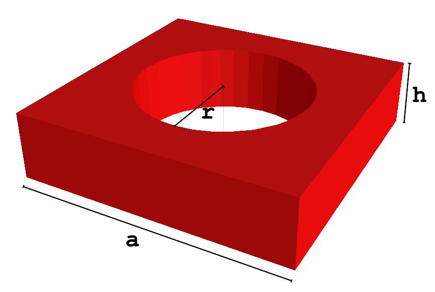
a, h and r labelled in a unit cell with a lattice constant of  , thickness of and hole radius of
  , defined with
 a=200, h=50 and r=65.The size and number of the individual hexahedral mesh elements making up the mesh is dependent on one of two parameters, e or s. Only one of the two should be given, as it is used with a to calculate the value for the other. (The mesh elements can be seen in Figure M4 as the smaller blue cubes.)
The number of mesh elements per unit cell side e always has three values, one for each dimension, with the first two being in the horizontal directions ( and ) and the third one in the vertical (). The total number of elements in a full membrane mesh is the product of the values of e. As the third value of e determines the number of “layers” of elements, it should be noted that the value cannot be smaller than the number of materials, since each layer of material must be represented by at least one layer of elements. Due to the construction of the periodic mesh, the first two values of e must be 3 or more. If the second value is left blank, the first value will be used for it (for instance e=8,,2 is equivalent to e=8,8,2), producing a square base.
If instead the component hexahedron preferred size s is used, a value for e is calculated such that each of the sides of a single undistorted element is as close as possible to the value of s in nanometers. Smaller values of s result in larger values of e. Since the finite element method grows better with increasing numbers of elements, the precision of the calculation (along with computation time) increases with larger values of e or smaller values of s.
3.2.2 Computational Parameters
The number of eigenvalues calculated is controlled with n. These (approximately) correspond to the lowest  eigenfrequencies in a given point in -space where is the value of
 n. (This is “approximate”, because the computed eigenvalues are not necessary ordered, essentially allowing some of the very highest computed values to “skip” eigenvalues.) Thus, whilst plotting a band structure, the very highest data points do not necessarily represent points on the same eigenmode, because the modes can overlap. It is therefore recommended to compute at least a few eigenvalues more than the desired minimum number of modes. Due to the manner of the eigenvalue solver SLEPc solving the eigenvalues, increasing the value of n increases computation times in steps.
The path and resolution of the -space sampling points are controlled with k, which always has two values. The first value is the IBZ path, specified by the three corner points of the IBZ triangle, , and , represented by standard ASCII characters G, X and M, respectively. Either a single corner point or a point-to-point route between the three points can be used. For instance, the input GXMG corresponds to the full path ") on the IBZ triangle. The second value of
on the IBZ triangle. The second value of k is the sampling resolution. It determines the number of points calculated, which are distributed evenly along the path. Because the full IBZ path is a right-angled isosceles triangle, the distribution of the points on the triangle sides –, – (the “catheti”) and – (the “hypotenuse”) is in the ratio  .
.
The computed points can also be “manually” set with the parameter K (uppercase), by specifying a file containing the desired -space coordinate points. This can be any number of points anywhere in -space, thus it may also include points inside the IBZ triangle. Therefore the K parameter has slightly more freedom than k.
The list of materials m should have the same number of values as h (the thicknesses of the materials). The names of the materials called must also be found in the material file materialParameters.txt, along with the material parameters lambda, mu and rho (respectively corresponding to , and from Equation NC1). For instance, silicon nitride Si3N4 can be called with m=Si3N4, should it be defined in the material file followingly:
    Si3N4:
        lambda=86.57 GPa
        mu=101.63 GPa
        rho=3100 kg/m3
3.2.3 Other Parameters
The verbosity level of the console output is controlled by p, with values ranging from 0 (nothing) to 3 (everything). S (uppercase) toggles snapping or “round-shifting”; with S=0 the hexahedral elements are not distorted and remain right-angled. Snapping is recommended to be toggled off for full membranes, but in meshes containing holes it will lead to “blocky” edges, as shown in Figure M4b, thus it may cause slightly smaller-than-intended radius. (Examples of round-shifting can also be seen in Figure M6.)
The symmetry of the (interior) mesh nodes can be broken with maximum lattice point random variation R (uppercase), whose values are in picometers. R=0 leaves the mesh unrandomized, any other value will cause the interior nodes to be randomly shifted that amount or less, in - and -direction. The overall shape of the mesh remains unchanged, as the border nodes are not disturbed (including the borders of the hole).
The visualization of the mesh is toggled with v, which requires an active GLVis server to be running. Boundary elements can be toggled with b and periodic borders with P (uppercase). However, these should only used for debugging purposes.
Parameters a, r, F and the components of h are of data type double and accept integer or decimal values. (Internally, these values are scaled to obtain best simulation precision for lattice constants with the order of magnitude near  , as seen in the console output described in Figure M3.) Parameters
 p, n, R, all components of e and the second component of k are of type int and accept only integer values. Parameters S, b, v and P behave like booleans and expect a value of 0 or 1 (corresponding to false or true, respectively). The string type parameters d (default settings file), all components of m and the first component of k should not contain spaces or commas in the string value (including filenames), as spaces are used to separate parameters and commas to separate parameter value components.
The command -help will show the description of exit codes, full list of parameters and the current default settings along with their comments.
3.2.4 Error States
Exit codes are implemented to enhance feedback for user in case of a fatal error. (The exit code is 0 when the program is run successfully.) The run is halted and a non-zero exit code is returned if some parameters would produce error states and prevent the program from running. As an example, trying to create a lattice with a hole too large to fit on the lattice would otherwise cause a crash (but instead returns exit code 8). In addition, a red warning message is displayed in the console (Figure M2). Below is a comprehensible list of non-zero exit codes:
    4: Material not found
    5: Material property not found
    6: Mismatch in number of materials and number of heights
    7: Too many undefined parameters
    8: Too big hole for the lattice
    9: Mismatch in number of vectors in the file and number
       given on the first line of the file
    10: Too few numbers of component elements
    11: Error in k-space sample file
    12: Error in k-space path or sampling resolution
    13: One of the parameters has been defined more than once
These exit codes were selected avoiding reserved exit codes. (E.g. exit code 1 is often used as a “general catchall” and exit code 2 for misuse of shell builtins). [Cooper-2014]
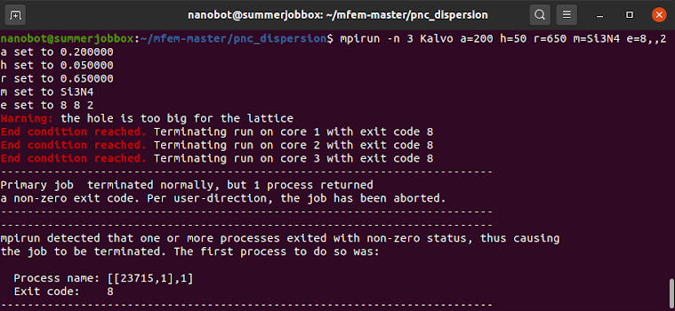
r=650) too large for the lattice constant (a=200) in the command prompt (the white text on the first line).3.3 Mesh
3.3.1 Mesh Generation
The mesh dimensions are based on the parameters for the lattice constant a and thickness h of the unit cell. The mesh consists of hexahedron-shaped elements, for which a parameter for either the per-dimension counts e or the preferred size s has to be provided. Based on the parameters, a rectangular cuboid mesh is generated from a number of small hexahedral elements, using the MeshFactory class.
First, a three-dimensional grid of vertices serving as the nodal points between the elements is created. (Because the vertices act as the corner points for the elements, the number of vertices per dimension is one greater than the number of elements per dimension.) The hexahedral elements with their corner points at the vertices are then created for all adjacent groups of 8 vertices, unless all 8 vertices of the hexahedron are bound within a cylinder with a radius of r from the center of the mesh. Thus, if r is greater than zero (and  ), a hole is left in the middle of the mesh, going from the top of the mesh all the way to the bottom.
Next, the innermost vertices are moved in - and -direction to be along the circumference of the hole (the “round-shifting”) and the remaining vertices are shifted outwards to enforce a more uniform size of a single element across the entire mesh. It should be noted however, that since the innermost hexahedrons are no longer cubical, the volume of an element near the edge can be more than twice as much as that of an inner element.
As an example, for a mesh with a lattice constant a=200, thickness h=50, radius of the hole r=65 and per-dimension element counts e=8,8,2, the number of initial vertices generated is \times(8+1)\times(2+1)=243") . In each layer of elements, there are 10 elements with each of their eight vertices within the range of the hole radius. Thus, (across the two layers) the total number of hexahedral elements created is
. In each layer of elements, there are 10 elements with each of their eight vertices within the range of the hole radius. Thus, (across the two layers) the total number of hexahedral elements created is \times2=108") . At this stage, all of the elements are still rectangular, and a “blueprint” of a this mesh is printed in the console using standard Unicode box-drawing characters (Figure M3).
. At this stage, all of the elements are still rectangular, and a “blueprint” of a this mesh is printed in the console using standard Unicode box-drawing characters (Figure M3).
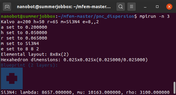
 base mesh with
 a=200, h=50 and r=65 printed in the bottom left-hand side of the console, corresponding to the mesh stage in Figure M4b. (Note that the displayed double type values set for a, h and r are scaled for the simulation and thus are not in nanometers internally.)Figure M4 visually demonstrates the evolution of this mesh base to the rough, angular hole and the eventual “round-shifting” of the hole borders. (It should be noted that code-wise, the hexahedral elements for the first visualized mesh with full  elements are not actually created, but only the vertices.) After the creation of the elements, the unused vertices are removed.
 mesh base, (b) the mesh without the twenty innermost elements and (c) the final mesh with the vertices shifted to circular shape and the surrounding elements adjusted accordingly (right). The mesh represents a unit cell with a lattice constant of , thickness of and a circular hole with a radius of
Quadrilateral boundaries are created on each of the exterior edges of the border hexahedrons. The border boundaries are attributed clockwise from 1 to 4. The top, bottom and the “inside” boundary of the cylindrical hole (if one exists) are all attributed 5. Any intermaterial boundaries within the mesh are attributed sequentially starting with 6. In order to make the mesh periodic, all boundaries of the first two horizontal edges are “fused” to the opposing side of the unit cell, i.e. 1 is connected to 3 and 2 to 4.
3.3.2 Precision
Tetrahedrons (convex 3D polytopes with four triangle faces, “triangular pyramids”) are often used for elements in three-dimensional meshes. In this software, hexahedrons were chosen to be used as the mesh elements because they can intuitively be used for a rectangular cuboid shaped unit cell without major drawbacks. If necessary, the symmetry can be broken through small adjustments to the vertices (with mesh randomness parameter R).
Matching test cases were created with COMSOL Multiphysics® to compare computed eigenvalues to those computed with Kalvo. The circular hole is approximated well, with precision increasing with more elements, as demonstrated Figure M5. In the mesh, the hole is a prism-like, near-regular polygon with rotational and reflection symmetry of order 4, as shown by in Figure M6.

 , for an
  base mesh of Al2O3 with
 a=200, h=50 and r=60 at ") in comparison to equivalent COMSOL Multiphysics® results with a
in comparison to equivalent COMSOL Multiphysics® results with a  base mesh. With
  the difference is below
  .
.
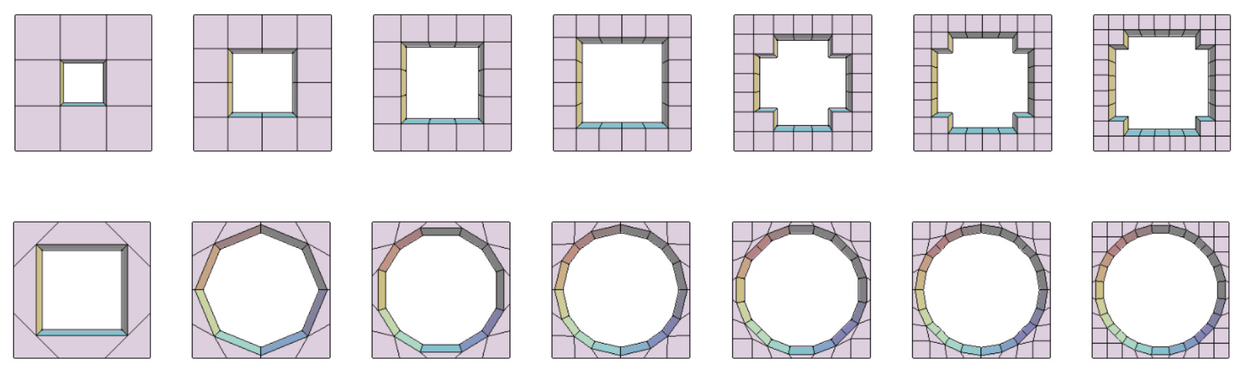
The downside of using hexahedral elements is that their faces are quadrilaterals. Unlike triangles, quadrilaterals can be non-convex polygons, the presence of which was noted to cause significant computational errors during physics simulation of the mesh. To avoid this, an algorithm was created to remove all concavity from the mesh. The algorithm is run before passing the mesh to the eigenvalue solver by shifting the problem vertices outwards from the center of the quadrilateral. Thus, all elements including the innermost hexahedrons in a hole-containing mesh have all of their interior angles less or equal to 180 degrees. As a result, the two-dimensional shape of the polygonal base of the hole is not necessarily strictly convex, but the scale of the concavity is negligible and does not influence computational accuracy.
3.4 Eigenvalue Solving
3.4.1 CLEEPS
The mesh is passed to the classical linear elastic eigenvalue problem solver (CLEEPS), which creates a parallel mesh of the serial mesh created with MeshFactory. Piece-wise constant coefficients of material parameters , and are created to account for the different materials in the mesh.
In CLEEPS, complex linear forms a and m are created with domain integrators for the non-derivative part (BlochVectorMassIntegrator), first derivatives (BlochGradientIntegrator) and second derivatives (ElasticityIntegrator) of the Equation NC1. The ElasticityIntegrator  \nabla u_j,\nabla v_i)") is an integrator found within the MFEM bilinear forms, but the other two were created specifically for this problem. [Lappalainen-Puurtinen-2021, Anderson-2021]
is an integrator found within the MFEM bilinear forms, but the other two were created specifically for this problem. [Lappalainen-Puurtinen-2021, Anderson-2021]
The BlochVectorMassIntegrator ") contains the non-derivative coefficients of the weak form of the Navier–Cauchy equation in a matrix form,
contains the non-derivative coefficients of the weak form of the Navier–Cauchy equation in a matrix form,
    DenseMatrix vmidm(3);
    {
        vmidm(0,0) = (lam+2*mu)*kx*kx + mu*ky*ky;
        vmidm(0,1) = (lam+mu)*kx*ky;
        vmidm(0,2) = 0;

        vmidm(1,0) = (lam+mu)*kx*ky;
        vmidm(1,1) = (lam+2*mu)*ky*ky + mu*kx*kx;
        vmidm(1,2) = 0;

        vmidm(2,0) = 0;
        vmidm(2,1) = 0;
        vmidm(2,2) = mu*(kx*kx+ky*ky);
    }
where variables lam, mu, kx and ky correspond to , , and , respectively. The first dimension of vmidm corresponds to the trial function dimension and the second to the test function dimension  , where (respectively corresponding to
 0,1,2 in code, due to indexing in C++). Thus, the first rows of each block of the matrix correspond to the coefficients in Equation W0.
Similarly, the coefficients in Equation W1 correspond to first blocks of the coefficient arrays in BlochGradientIntegrator ") ,
,
    MQpos[0][0][0] = (lam+2*mu)*kx;
    MQpos[0][0][1] = mu*ky;
    MQpos[0][0][2] = 0;
    MQpos[0][1][0] = lam*ky;
    MQpos[0][1][1] = mu*kx;
    MQpos[0][1][2] = 0;
    MQpos[0][2][0] = 0;
    MQpos[0][2][1] = 0;
    MQpos[0][2][2] = mu*kx;

    MQneg[0][0][0] = -(lam+2*mu)*kx;
    MQneg[0][0][1] = -mu*ky;
    MQneg[0][0][2] = 0;
    MQneg[0][1][0] = -mu*ky;
    MQneg[0][1][1] = -lam*kx;
    MQneg[0][1][2] = 0;
    MQneg[0][2][0] = 0;
    MQneg[0][2][1] = 0;
    MQneg[0][2][2] = -lam*kx;
where MQpos and MQneg are three-dimensional arrays. In both arrays, the first dimension of the array corresponds to the test function dimension and the second to the trial function dimension . The third dimension of the array corresponds to the test function derivative direction  in
in MQPos and to the trial function derivative direction  in
in MQNeg, where  (corresponding to
 0,1,2 in code). For instance, MQpos[0][1][2] corresponds to the coefficient of the term  , which is
  .
.
The integrators create an mfem::DenseMatrix type element matrix consisting of submatrices calculated with the aforementioned coefficients in their AssembleElementMatrix subroutine. After initializing the integrators, matrices A and M are then created that define the generalized eigenvalue problem }}
\end{equation}") where
where  corresponds to in Equation G1. This is done by forming
 ParSesquilinearForm type pointers, combining the element matrices of all integrators with their Assemble subroutine and eventually using them to create PetscParMatrix type system matrices that are passed to the SLEPc solver. (Due to restrictions in implementing complex numbers with MFEM at the time of writing the code, the system matrix consists of real numbers representing the real and imaginary parts.) [Falgout-Yang-2002, Balay-2021]
From Equation G2, the is solved for a number of eigenvalues and the  is obtained by taking the square root of , thus the frequency is
  . (A scaling coefficient is also used for unit conversion.) This is repeated for all desired -space values. (As a side effect of segregating the real and imaginary parts in the PETSc system matrix, all eigenvalues are technically doubled redundantly, but only the eigenvalues with an odd index are saved, effectively ignoring every other value.)
3.4.2 Output
The program outputs a text file with all the eigenvalues. The name of the file consists of four items: the list of materials separated by comma, the lattice constant, the heights of the materials separated by comma and the radius of the hole. The four items are separated by underscore and the last three items preceded by their one-character parameter symbols, a, h and r, respectively.
The first line of the file is the number of eigenfrequencies per point in -space. All remaining lines consist of the coordinate points in -space ( and separated by comma), each immediately followed by the eigenfrequencies (in  ) solved for the point, each on their own line. For instance, for the Si3N4 mesh in Figure M4 with
 n=5 and k=GXMG,50, the generated file Si3N4_a200_h50_r65.txt begins followingly:
5
0,0
-nan
-nan
-nan
1.29829e+10
1.32996e+10
1.0472,0
5.9531e+08
1.95354e+07
1.26717e+09
1.25302e+10
1.29985e+10
2.0944,0
7.80578e+07
  ...
Here, the first line (5) is the number of eigenvalues, the second line (0,0) is the first point in -space (with  and
and  ), the next five lines are the solved frequencies at that point, the 8th line (
1.0472,0) is the second point in -space, and so on.
Due to the computational method used, the eigenfrequencies are in no particular order. Very small frequencies (below  ) sometimes show as
 nan or -nan (“not a number”), because near-zero values can be negative within the computational accuracy and solving from Equation G2 requires taking a square root. (Square roots of negative numbers are not defined a number value in the double date type.) This usually only affects the first three values at . (The nan/-nan values are marked as in the example Python plotter file in Appendix 2.)
It should be noted that (unless renamed) the eigenvalue text file will be overwritten if a mesh with identical geometry and material parameters is created, because it will have the same filename (even if there is a change in another parameter, such as e). In addition, the latest created mesh is always saved in pnc.mesh file (encoded with the general MFEM mesh format MFEM mesh v1.x). This mesh file, unless renamed, is overwritten on every run. This is intended behaviour to reduce redundant disc space usage. [Kolev-Dobrev-2010]
3.4.3 Efficiency
For a mesh with mesh base of  elements, where is the number of elements in (horizonal) - and -dimension and in (vertical) -dimension, the runtime of the program increases about quadratically as a function of , as witnessed in Figure T1. increases the runtime about linearly. When looking for band gaps, a good balance between efficiency and precision can be achieved, for instance, with of 15. For two-material meshes, of 5 is usually the smallest sufficient number of vertical elements, if one of the materials is significantly thinner than the other.
 , for solving the eigenvalue problem for the base mesh used in Figure M5 with Jyväskylä FGCI (Finnish Grid and Cloud Infrastructure) Clusters puck.
The time spent on creating the mesh is negligible and most of the computation time is spent on solving the eigenvalue problem in each -space point. A fraction of this time is spent on forming the matrix, whilst obtaining the eigenvalues with SLEPc takes the longest.
The number of eigenvalues solved increases the computation time of the program near-linearly up to 250 eigenvalues, after which the computation time increases in steps of 40 to 70 eigenvalues (excluding the first step size), as shown in Figure T2. This is typical behaviour for the SLEPc eigenvalue solver. (Interestingly, solving 250–263 eigenvalues is faster than solving 249 eigenvalues.) [Roman-2021]
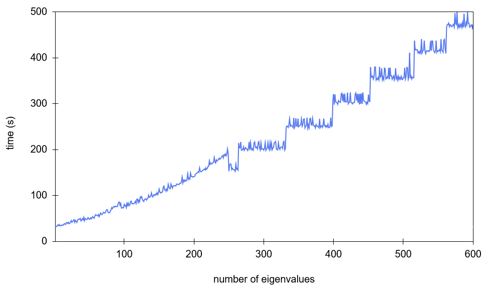
 base mesh with Jyväskylä FGCI Clusters puck. The time increase is initially about linear as a function of the number of eigenvalues, but after 250 eigenvalues the time increases in steps.
The speedup gained from using a large number of parallel processes can depend on many things, such as other simultaneous processes and the hardware used. On the Jyväskylä FGCI (Finnish Grid and Cloud Infrastructure) Clusters puck, the speedup behaves near-linearly up to 4 parallel processes, as demonstrated by Figure T3. After 20 parallel processes, the speedup decreases significantly. Therefore, it is more efficient to, for instance, run two simultaneous jobs with 8 parallel processes each, rather than run the two jobs back-to-back with 16 parallel processes.
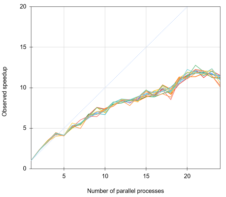 base mesh for different number of parallel processes for 10 different runs (coloured curves) as a function of the number of parallel processes, with the blue dashed line showing the optimal speedup. For all these runs, linear scaling (or apparent super-linear scaling) can be observed until 4 parallel processes, after which the rate of speedup decreases significantly. The measurements were performed on the Jyväskylä FGCI Clusters puck.
Simulating a  base mesh for 50 eigenvalues with a sampling rate of 60, takes about 50 minutes with Jyväskylä FGCI Clusters puck using eight parallel processes, in 2021.
4. Research and Results
All results presented from hereon use a mesh base of  elements or more. Thus, concluding from the comparison in Figure M5, all values computed from the simulations have a computational uncertainty of
  or less. The simulations were performed on the Jyväskylä FGCI Clusters puck. The values of the material parameters used in the simulations are listed in Appendix 3, in the format they appear in the
 materialParameters.txt file (with Lamé parameters calculated according to Equation NC2). [Lide-2005, Nunes-1990]
Referring to the eigenmodes is made difficult by the nature of the band structure; the modes intersect and change order as they are shifted by changing parameters. In the following sections, referring to the “th mode” means the eigenmode with the th lowest frequency at the indicated point in -space.
4.1 Band Gaps in Pure Silicon Nitride Phononic Crystals
4.1.1 Prior Work
In 2014, Zen et al. engineered thermal conductance with FEM simulations of phononic crystals. FEM band structure calculations showed that for a Si3N4 phononic crystal with a large cylindrical hole (filling factor of ), there is a large band gap with relation to the thickness, when thickness to lattice constant ratio is  [Zen-2014]
 of , thickness of and filling factor of (equating radius of
  and
and  ). The band gap is highlighted in red.
Moreover, their simulations also showed a band gap of similar magnitude at a lower frequency, when  This has the potential of having a larger band gap width-to-midpoint ratio (
 ), from hereon referred to as the “relative band gap”, which is more relevant than the absolute width of the band gap, since the band structure can be scaled by inversely scaling the all dimensions of the unit cell. By simulating this structure with Kalvo, for a lattice with lattice constant of , matching results were discovered (Figure R1); there is a band gap of
  with midpoint at
  , which equates to .
Broadly speaking, bigger relative band gaps are more interesting. The width of the band gap in Figure R1 is limited by the 6th eigenmode at from below and by the 7th mode at from above. If these modes can be shifted down and up, respectively, the band gap will increase in width. (Performing this is discussed after the next section.)
4.1.2 Modes Visualized
The software has also rudimentary support for visualizing the eigenmodes in a point in -space by sending the computed eigenvalues and displacements in the grid function by socket to a GLVis server. [Kolev-2010].
Figure R1 uses a sampling resolution of 60 points, 19 of which are used for the – section of the full IBZ path. (18, excluding the initial point at , the “zeroth” point.) For the first 25 modes, there are no intersecting modes at one third of the way from to , with all modes being relatively well spread from each other, thus they can easily be told apart. On the – path,  for all values and
  at . Hence, a point for visualization was selected at
  With the 18 points this corresponds to the 6th set of eigenfrequency data points in Figure R1, at
 ") . This is highlighted in Figure R2.
. This is highlighted in Figure R2.
 – section of the band structure for Si3N4 phononic crystal with lattice constant of , thickness of and filling factor of . A vertical yellow bar indicates the set of data points at
  = (6\pi /18a,0) \approx (1.0472/a,0)") .
.When it comes to the shape of the modes, the exponent term of the trial function causes a phase shift in different points. Figure R3 visualizes the real solutions of lowest six modes at . In a full membrane, the lowest three modes, the flexural, shear and longitudinal modes, oscillate in -, - and -axis, respectively. For the Si3N4 phononic crystal with lattice constant of , thickness of and filling factor of , the lowest three modes mainly oscillate correspondingly, with the waves propagating towards positive . The fourth mode twists torsionally about the -axis with rotational symmetry of order 4. The modes 5 and 6 with transverse wave motion are very similar to one another, apart from oscillating in - and -axis, respectively. [Muhammad-Lim-2020]
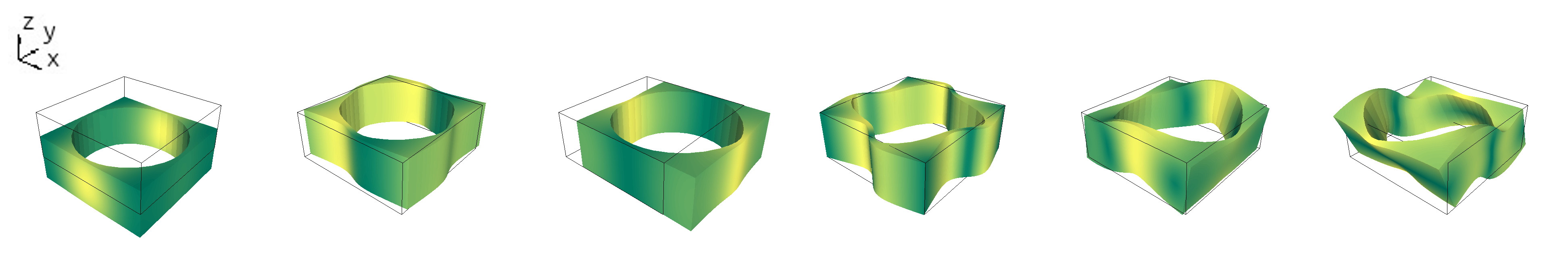 , thickness of and filling factor of at -space point . The black-edged box represents the initial state of the unit cell.
Figure R4 visualizes modes “7–12”, the lowest six modes immediately above the band gap. Mode 7 oscillates along the -axis, very similar to mode 8, oscillating along the -axis. However, in mode 8 the oscillation is in the same phase along the oscillation axis, but in mode 7 it is not. (This similarity/difference is difficult to see in the GLVis still image visualizations, which are in different phases with each other due to technical limitations.) Modes 10 and 11 exhibit similar pair-wise oscillation to modes 7 and 8, with mode 10 oscillating in phase along the -axis and mode 11 oscillating out of phase along -axis. Mode 9 oscillates in all axes, with waves propagating towards positive . Mode 12 has a circular oscillation about the -axis.
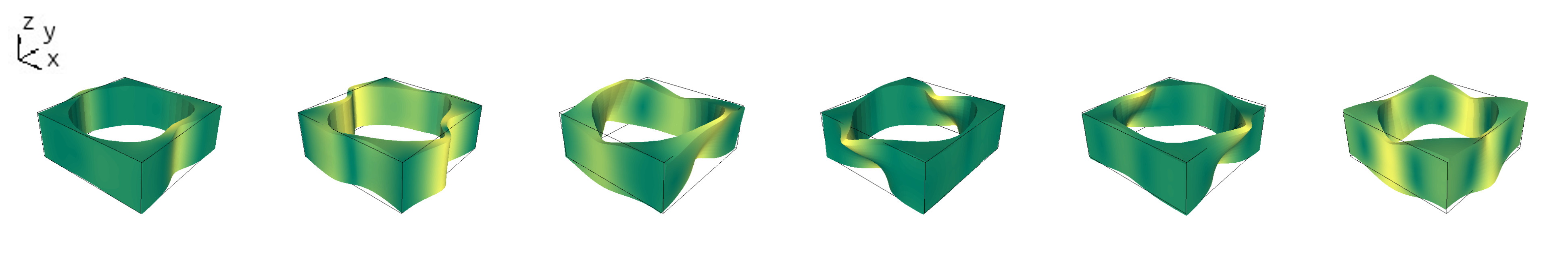 , thickness of and filling factor of at -space point .
4.2 Band Gaps in Multilayered Si3N4 Based Phononic Crystals
4.2.1 Si3N4–Al2O3 Dual Layer Membranes
Since the eigenmodes behave differently for different structures and different materials, the band structure of the silicon nitride phononic crystal in Figure R1 can be changed by adding a layer of another material on top of it. (Whether the second material is on top or on bottom of the first one, is irrelevant; the band structure in the horizontal IBZ is independent of the vertical orientation.)
Simulations showed that adding a layer of polystyrene (PS), a soft material, did not significantly increase the relative band gap. On the other hand, adding a layer of lead (Pb), a hard material, immediately shifted down all higher modes, effectively reducing the relative band gap, too. However, a layer of aluminum oxide (Al2O3) yielded some promising results.
Since the software can be executed with command prompts, it is easy to go through different structures by writing a Bash script with a loop. The lattice in Figure R1 was stacked with a layer of Al2O3, creating a Si3N4–Al2O3 dual layer membrane. Keeping the thickness of the Si3N4 layer constant (), varying thicknesses of Al2O3 were looped over. Figure R5 shows select band structures for a silicon nitride aluminum oxide dual layer membrane.
As the thickness of the layer of Al2O3 increases, the mode immediately above the band gap (starting at \approx\SI{3.5}{GHz}") ) for
) for  , is shifted up, causing the bad gap to rapidly widen until the gap is met with the next mode above it (when
  ). This next mode also shifts up, but more slowly, especially at IBZ point , where the band gap is now limited at instead of at .
The sixth mode at (starting at \approx\SI{2.7}{GHz}") immediately below the band gap) also initially shifts upwards, but starts shifting down after the thickness of Al2O3 grows above
immediately below the band gap) also initially shifts upwards, but starts shifting down after the thickness of Al2O3 grows above  . Hence, the band gap is limited less from below at IBZ -space point , causing the lower bound of the band gap to start decreasing rapidly and consequently starting the widening of the band gap.
The 10th mode at (the fourth one up from the band gap when  , starting at
 \approx\SI{4.5}{GHz}") ) shifts down as the thickness of Al2O3 increases. It “reaches” the band gap at IBZ point when
) shifts down as the thickness of Al2O3 increases. It “reaches” the band gap at IBZ point when 
 , stopping the widening of the band gap after that point. This is because the upper bound of the band gap goes down in frequency faster than the lower bound. This behaviour can clearly be seen in Figure R6, which visualizes the upper and lower boundaries of the band gaps as a function of Al2O3 thickness.
Thus, for Si3N4–Al2O3 dual layer membrane with , the largest relative band gap,  , is achieved with
  . This can be observed in the maximum of the bright blue undashed curve on the left-hand side of Figure R7
 and filling factor of , with a thick layer of Si3N4, for varying thicknesses of an Al2O3 layer. (The blue data points represent the upper and lower bounds of the band gap.) The sizes of the corresponding relative band gaps are plotted by the solid bright blue curve in Figure R7.
Adding the layer of Al2O3 on top of the Si3N4 membrane naturally increases the total thickness of the membrane, thus somewhat limiting the membrane’s potential for large band gaps. Hence, adding the layer of Al2O3 was simulated on varying thicknesses of Si3N4 (with a sampling resolution of  ), presented in Figure R7 (visualized with a selectively lower sampling resolution, for the sake of clarity). For this dual layer membrane with a filling factor of , the highest relative band gap,
  , is achieved with of
  (plotted by the black undashed curve) when , making the total thickness of the membrane
  .
.
Figure R7 also shows another local maximum of  for around of (solid red curve) when =
 , making the total thickness of the membrane
  . This shows that, for this phononic crystal structure, Si3N4–Al2O3 dual layer membrane produces larger relative band gaps than pure Si3N4 or Al2O3 membranes. For pure Al2O3 (the rightmost, violet curve), the largest relative band gap of
  is produced with =
 .
.
 and filling factor of . The highest relative band gap is achieved with = (the solid black curve) when =
 .
.4.2.2 Triple Layer Membranes
In terms of the simulations, there is no difference in the order of the materials in a dual layer membrane (i.e. Si3N4–Al2O3 = Al2O3–Si3N4). Triple layer membranes were tested by vertically surrounding the Si3N4 with another material from both top and bottom, and vice versa, to find out the effect of dividing one material into two (under and over the other material in the middle).
 and
and  (left), Al2O3–Si3N4–Al2O3 triple layer membrane with respective layer thicknesses of
  , and
, and  (middle) and Si3N4–Al2O3-Si3N4 triple layer membrane with respective layer thicknesses of
  ,
,  and (right). All three membranes have a total thickness of
  with Al2O3 to Si3N4 ratio of , lattice constant of and filling factor of .
Figure R8 shows the band structures for three membranes:
a Si3N4–Al2O3 dual layer membrane with respective layer thicknesses of
and ,an Al2O3–Si3N4–Al2O3 triple layer membrane with respective layer thicknesses of
, and , anda Si3N4–Al2O3-Si3N4 triple layer membrane with respective layer thicknesses of
, and .
(Hence, each membrane has a total thickness of and Al2O3 to Si3N4 ratio of .) For the first two (Si3N4–Al2O3 and Al2O3–Si3N4–Al2O3), the frequencies of individual data points in the band structures are identical within . (However, this does not mean that the modes are unchanged.) With Al2O3 in the middle, between two layers of Si3N4 (Si3N4–Al2O3-Si3N4), the differences are more pronounced.
Polystyrene also exhibited slightly similar behaviour as Al2O3, with Si3N4–PS–Si3N4 band structures being very different to Si3N4–PS and PS–Si3N4–PS band structures, even losing the band gap of the membrane with to ratio of (Figure R9). This difference can be explained with Si3N4 being significantly denser and stiffer than polystyrene, whereas Si3N4 and Al2O3, in comparison, have very similar material parameters altogether.
 and (left), PS–Si3N4–PS triple layer membrane with respective layer thicknesses of , and (middle) and Si3N4–PS-Si3N4 triple layer membrane with respective layer thicknesses of , and (right). All three membranes have a total thickness of with PS to Si3N4 ratio of , lattice constant of and filling factor of .
The difference between the Si3N4–PS dual and triple layer membranes grows larger when the to ratio increases. The band gap still exists for Si3N4–PS–Si3N4 membrane with to ratio of  . For both Al2O3 and PS, three of the lowest six modes (namely 2nd, 3rd and 5th modes) remain almost unchanged between the dual and triple layer membranes, whilst the higher modes are reduced for the configuration with the stiffer material on top and bottom.
As a somewhat analogous macroscopic example, a leather wallet with payment cards inside can be considered a soft–hard–soft triple layer membrane. If instead the bare leather is sandwiched between the hard cards, the new hard–soft–hard structure stretches similarly as before, but does not bend as easily. In Figure R9, the two “linear” modes near , the shear and longitudinal modes, remain nearly unchanged, whilst the 1st mode, the flexural mode, sees a large change in the third band structure.
4.3 Effect of Filling Factor
Increasing the filling factor by increasing the radius of the cylindrical hole widens the band gap. The theoretical maximum for the radius is half of the lattice constant, equating to a filling factor of . (This would mean zero-diameter walls between the holes!) However, according to experiences in the Nanoscience Center at the University of Jyväskylä, walls with a diameter smaller than are difficult to create in practice and tend to be too fragile. [Loippo-2019]
All of the lower modes in the band structure are shifted down when the radius increases, constricting the band gap less and thus increasing its width. Figure R10 shows how the lower modes shift down at a higher rate than modes immediately above the band gap when the radius of the hole is increased. For Si3N4–Al2O3 dual layer membrane with respective layer thicknesses of  and and lattice constant of , the highest low mode’s maximum at is at a higher frequency than the minimum of the lowest of the upper modes at , when the radius is below
  (corresponding to filling factor of
  ), and the band gap does not exist on radii approximately smaller than or equal to that.
This behaviour is also clearly visible in Figure R11 which visualizes the upper and lower boundaries of the band gaps as a function of radius . The width of the band gap increases rapidly with increasing radius, up until for values with  , which have the upper boundary of the band gap constricted by a mode minimum at . For a lattice constant of , this radius corresponds to a filling factor of
 , thickness of the Si3N4 layer of and thickness of the Al2O3 layer of as a function of the radius of the cylindrical hole. The blue data points represent the upper and lower bounds of the band gap. The upper bound of the band gap reaches its maximum at
  (
( ). The band gap does not exist when
  (
( ). However, the exact point is not rendered in the graph, because the used sampling resolution of the radius is at that point.
Appendix 1 is an example of a Bash script used to conduct such a systematic study of varying the radius of the hole (from to  with a sampling resolution of ) in a dual layer phononic crystal membrane with a
 for loop. In 2021, executing the script with eight parallel processes on the Jyväskylä FGCI Clusters puck takes about eight hours.
5. Conclusions
In this work, a software was developed for simulating the dispersions of multilayered phononic crystals with cylindrical hole lattice, utilizing MFEM and SLEPc libraries. The software was tested for a systematic study of structures with single- and multimaterial membranes, by starting with a known single-layer phononic crystal membrane and systematically optimizing the structure to find new multilayered membranes with larger band gaps, using materials commonly used in the laboratory. The properties of these newfound multilayer membranes have not been experimentally verified. The computation was performed on structures with the order of magnitude in nanometers, but the structures can be scaled to smaller or larger scales.
As a starting point, matching results about Si3N4 phononic crystal were found with the study by Zen et al. in 2014; a thick Si3N4 membrane with a lattice constant and a filling factor of has a relative band gap of . Through systematic study, it was discovered that this relative band gap can be enlargened to  by adding a layer of Al2O3 on top of it. The Si3N4–Al2O3 dual layer membrane’s relative band gap is the largest,
  , when = and =, with the total thickness of the membrane at .
It was also shown that increasing the filling factor increases the width of the band gap, but there is a clear point where diminishing returns become very high. For this configuration of materials  and
and ") , the band gap appears when the filling factor is above , increasing rapidly until a filling factor of
, the band gap appears when the filling factor is above , increasing rapidly until a filling factor of  . This suggests that in order to develop a desired band gap, after a certain point it may be more effective to scale the entire unit cell as opposed to increasing the filling factor that also comes with the cost of reducing the diameter of the walls between the holes. Very thin walls are difficult to fabricate and can reduce the structural integrity of the material.
The relative band gap of the Si3N4–Al2O3 dual layer membrane was larger than for pure Al2O3, showing that a dual layer membrane can yield a larger relative band gaps than its component materials alone. It was also found that the band structure changes if one of the two materials is instead distributed into two layers surrounding the other material, especially if the distributed material is the stiffer of the two. Si3N4–PS and PS-Si3N4–PS membranes with to ratio of and have a band gap whereas the corresponding Si3N4–PS–Si3N4 membrane does not. The Si3N4 membrane’s band gap could not be increased with PS or Pb.
For all simulations performed, the local maxima and minima of individual modes that restrict the band gap are always located at the corner points of the IBZ triangle (at , or ). However, a few non-intervening local minima of the high frequency modes can be observed outside the corner points, especially between and . It can therefore be concluded that using a sampling resolution of 3 alone, thus plotting only the corner points, is not a reliable method for finding band gaps, as it could result in false positives. That said, no such band gap affecting modes came across during this study, thus a sampling resolution of 3 (with intermediate point linear interpolation) could certainly be used to quickly eliminate band structures without band gaps, only to later filter out false positives with a higher sampling resolution.
Furthermore, the results of the software match those acquired with the commercial mathematical modelling software COMSOL Multiphysics® to a high degree, whilst allowing looping over parameters using Bash scripts, hence being extremely faster for this type of task. As thousands of files were generated throughout this work, during the data analysis, the naming convention used in the filenames produced by the software also proved to be very good for quickly finding and comparing certain structures from the massive set of data that was computed, using the file names as the search term. Additionally, the mode visualizations can be used in the analysis.
The software has shown to be useful in studying the dispersive properties of phononic crystals, as it can be used to rapidly analyze multiple varying structures. By changing one parameter and going through the multiple structures, such systematic study can easily be conducted. Appendix 1 is an example Bash script for looping over radii (as shown in Figure R10) with an example Python plotter in Appendix 2.
5.1 Future Work
The software is currently limited to computing full membranes and membranes with a cylindrical hole of constant radius throughout the entirety of the rectangular unit cell. In practice, the cylindrical holes rarely have a constant radius, thus an upcoming feature is the support for holes in the shape of a conical frustum (a cylinder with different top and bottom radii,  and
and  ). The implementation of this feature is mostly done and will work similarly to the lattice constant parameter
 a, with two input values of r corresponding to and , and one input value signifying a constant radius .
Another future feature is the exclusion of the hole from a number of the material layers, resulting a multilayered material with a hole through only some of its layers. This is instrumental for adding the support for pillar structures, which in addition to hole phononic crystals, also provide interesting dispersion spectrums. In the pillar structures, protruding bodies of material sit atop of full membrane of the same or another material. Adding this feature simply requires implementation of the aforementioned hole exclusion and “flipping” the geometry of the hole by not creating elements with their vertices outside the given radius, as opposed to ones inside the radius. Support for rectangular holes/pillars will also be added.
The rectangular unit cell used in the software can only simulate phononic crystals in a rectangular grid arrangement. In order to simulate other grids, such as hexagonal grids, the shape of the unit cell must also be of different shape. For a hexagonal unit cell however, element shapes other than the hexahedron may have to be considered.
At the time of coding the CLEEPS class, MFEM had no support for complex numbers. Because of this, the large PETSc system matrix passed to the SLEPc eigenvalue solver is created from real numbers representing the real and imaginary parts of the complex number. As a result, all eigenvalues are redundantly computed twice, which could be optimized to speed up computation with the newly added complex number support in MFEM.
As the software can be run entirely by giving the desired parameters upon execution, it is an excellent “backend” for a graphical user interface (GUI). With a GUI front end, the user could observe the development of the band structure as it gets refined with data points as the program is running and updating the diagram. This allows the user to quickly test different parameters and halt the computation if the band structure becomes uninteresting. A real-time visualization is technically possible in the current version, as the output text file is appended throughout the simulation as more points in -space are computed. However, the computations occur in the order the -space points appear in the defined IBZ path, if a -space file is not specified. The band structure diagram refining in real time would be best utilized with an order that starts with a low sampling resolution (such as the one shown in Figure D4) and then iteratively fills in the points between the computed points.
Lastly, it would be possible to automate a task, such as finding band gaps, with machine learning. Hybrid machine learning algorithms have recently been applied for the prediction of the thermal conductivity of nanocomposites by Liu et al. in 2021. Kalvo’s easy executability with Bash scripts allows for the generation of a huge amount of desired training data, which can be used for the machine learning algorithm to build a model on the behaviour of the modes. [Liu-2021]
Bibliography
- [Anderson-2021]: R. Anderson et al., “MFEM: A Modular Finite Element Library”, In: Computers & Mathematics with Applications, 81 (202), pp. 42-74, DOI: 10.1016/j.camwa.2020.06.009.
- [Balay-2021]: Satish Balay et al., “PETSc/TAO Users Manual”, (202), Argonne National Laboratory, ANL-21/39 - Revision 3.16, URL: https://petsc.org/ (visited on 2021-10-14).
- [Comsol-2020]: “COMSOL Multiphysics® v. 5.6.”, (2020), COMSOL AB, Stockholm, Sweden, URL: https://www.comsol.com/ (visited on 2021-10-12).
- [Cooper-2014]: Mendel Cooper, “Advanced Bash-Scripting Guide, Appendix E. Exit Codes With Special Meaning”, (2014), The Linux Documentation Project, URL: https://tldp.org/LDP/abs/html/exitcodes.html (visited on 2021-06-0).
- [Cui-2014]: Tie Jun Cui et al., “Coding metamaterials, digital metamaterials and programmable metamaterial”, In: Light: Science & Applications, 3 (2014), p. e218, DOI: 10.1038/lsa.2014.99.
- [Falgout-Yang-2002]: Robert D. Falgout and Ulrike Meier Yang, “hypre: A Library of High Performance Preconditioners”, In: Computational Science — ICCS 2002, 2331 (2002), pp. 632-641, Springer, Berlin, Heidelberg, DOI: 10.1007/3-540-47789-6_66.
- [Gabriel-2004]: Edgar Gabriel et al., “Proceedings, 11th European PVM/MPI Users’ Group Meetin”, pp. 97–104, Budapest, Hungary, Septembe.
- [Garcia-Alvarez-2015]: Pablo Gómez García and José-Paulino Fernández-Álvarez, “Floquet-Bloch Theory and Its Application to the Dispersion Curves of Nonperiodic Layered System”, In: Mathematical Problems in Engineering, 2015 (2015), DOI: 10.1155/2015/475364.
- [Ibach-Luth-2009]: Harald Ibach and Hans Lüth, “Solid State Physics: An Introduction to Principles of Materials Scienc”, (2009), Springer, London, New Yor.
- [Jia-2018]: Zian Jia et al., “Designing Phononic Crystals with Wide and Robust Band Gaps”, In: Physical Review Applied, 9 (2018), p. 044021, DOI: 10.1103/PhysRevApplied.9.044021.
- [Karypis-Kumar-1999]: George Karypis and Vipin Kumar, “A Fast and Highly Quality Multilevel Scheme for Partitioning Irregular Graph”, In: SIAM Journal on Scientific Computing, 20 (1) (1999), pp. 359-392, Springer, Berlin, Heidelberg.
- [Kittel-1996]: Charles Kittel, “Introduction to Solid State Physics”, (1996), John Wiley & Sons, Inc., US.
- [Kolev-2010]: Tzanio Kolev and Veselin Dobrev, “GLVis: OpenGL Finite Element Visualization Tool”, (2010), USDOE, Lawrence Livermore National Laboratory, DOI: 10.11578/dc.20171025.1249, URL: https://glvis.org/ (visited on 2021-10-12).
- [Kolev-Dobrev-2010]: Tzanio Kolev and Veselin Dobrev, “MFEM: Modular Finite Element Methods [Software]”, (2010), USDOE, Lawrence Livermore National Laboratory (LLNL), Livermore, CA (United States, DOI: 10.11578/dc.20171025.1248, URL: https://mfem.org/ (visited on 2021-10-12).
- [Lappalainen-Puurtinen-2021]: Panu Lappalainen and Tuomas Puurtinen, “GitLab repository of Kalvo (PnC dispersion)”, University of Jyväskylä, URL: https://gitlab.com/nanopnc/pnc_dispersion (visited on 2021-08-0).
- [Laude-2020]: Vincent Laude, “Phononic Crystals”, (2020), De Gruyter, Berlin/Bosto.
- [Li-Wen-Sheng-2021]: Jensen Li et al., “Acoustic metamaterials”, In: Journal of Applied Physics, 129, 171103 (2021), DOI: 10.1063/5.0046878.
- [Lide-2005]: David R. Lide, “CRC Handbook of Chemistry and Physics, Internet Version 2005”, (2005), CRC Press LLC, Boca Raton, Florida, USA.
- [Liu-2021]: Bokai Liu et al., “A stochastic multiscale method for the prediction of the thermal conductivity of Polymer nanocomposites through hybrid machine learning algorithm”, In: Composite Structures, 273 (2021), p. 114269, DOI: 10.1016/j.compstruct.2021.114269.
- [Loippo-2019]: Teemu Loippo, “2D phonon thermal transport in thin SiN film”, (2019), Department of Physics, University of Jyväskylä, URL: http://urn.fi/URN:NBN:fi:jyu-201904032052 (visited on 2021-10-12).
- [Lucklum-Vellekoop-2017]: Frieder Lucklum and Michael J. Vellekoop, “Design and Fabrication Challenges for Millimeter-Scale Three-Dimensional Phononic Crystal”, In: Crystals, 7 (11) (2017), p. 348, DOI: doi:10.3390/cryst7110348.
- [Mendez-2017]: Carlos Gustavo Méndez et al., “Computational material design for acoustic cloaking”, In: International Journal for Numerical Methods in Engineering, 112, 10 (2017), pp. 1353-1380, DOI: 10.1002/nme.5560.
- [Muhammad-Lim-2020]: Muhammad and C. W. Lim, “Analytical modeling and computational analysis on topological properties of 1-D phononic crystals in elastic medi”, In: Journal of Mechanics of Materials and Structures, 15 (1) (2020), pp. 15-35, DOI: 10.2140/jomms.2020.15.15.
- [Nunes-1990]: Rafael Nunes et al., “ASM Handbook, Volume 2, Properties and Selection: Nonferrous Alloys and Special-Purpose Material”, (1990), ASM International, USA.
- [Palermo-Marzani-2020]: Antonio Palermo and Alessandro Marzani, “A reduced Bloch operator finite element method for fast calculation of elastic complex band structure”, In: International Journal of Solids and Structures, 191-192 (2020), pp. 601-613, DOI: 10.1016/j.ijsolstr.2019.12.011.
- [Puurtinen-2020]: T. A. Puurtinen et al., “A Composite Phononic Crystal Design for Quasiparticle Lifetime Enhancement in Kinetic Inductance Detecto”, In: Journal of Low Temperature Physics, 199 (2020), p. 577–584, DOI: 10.1007/s10909-020-02423-4.
- [Ramsay-1958]: John F. Ramsay, “Microwave Antenna and Waveguide Techniques before 1900”, In: Proceedings of the IRE, 46 (2) (1958), pp. 405-415, DOI: 10.1109/JRPROC.1958.286869.
- [Roman-2021]: Jose E. Roman et al., “SLEPc Users Manual - Scalable Library for Eigenvalue Problem Computation”, (2021), Universitat Politecnica de Valencia, URL: https://slepc.upv.es/documentation/slepc.pdf (visited on 2021-06-1).
- [Royer-Dieulesaint-2000]: Daniel Royer and Eugéne Dieulesaint, “Elastic Waves in Solids I: Free and Guided Propagation”, (2000), Springer, Heidelberg, German.
- [Strauss-2007]: Walter A. Strauss, “Partial Differential Equations: An Introduction”, (2007), John Wiley & Sons, River Street, Hoboke.
- [Tian-2016]: Yolan Tian, “Studies of two-dimensional and three-dimensional phononic crystal structure”, (2016), Research report, Department of Physics, University of Jyväskylä, URL: http://urn.fi/URN:ISBN:978-951-39-6702-4 (visited on 2021-10-12).
- [Zen-2014]: Nobuyuki Zen et al., “Engineering thermal conductance using a two-dimensional phononic crysta”, In: Nature Communications, 5 (2014), DOI: 10.1038/ncomms4435.
- [Zienkiewicz-1977]: O. C. Zienkiewicz, “The Finite Element Method, Third edition”, (1977), McGraw-Hill Book Company (UK) Limited, Maidenhead, Berkshire, Englan.
- [Zienkiewicz-2013]: O. C. Zienkiewicz et al., “The Finite Element Method: Its Basis and Fundamentals, Seventh editio”, (2013), Butterworth-Heineman, Oxford, U.
- [Zienkiewicz-Morgan-1983]: O. C. Zienkiewicz and K. Morgan, “Finite Elements and Approximation”, (1983), John Wiley & Sons, Inc., US.
Appendices
Appendix 1: Bash Iterator for Radius
#!/bin/bash
# @author Panu Lappalainen
# @version 210829
# Example Bash script that loops over varying radii with Kalvo
# and plots the band structure with a Python plotter Plotter.py

A=1000 # lattice constant
E=15,,5 # mesh element counts (x,y,z)
M=Si3N4,Al2O3 # list of materials
H1=340 # thickness of 1st layer
H2=130 # thickness of 2nd layer
N=50 # number of eigenvalues
KPATH=GXMG # k-space path in IBZ
KCOUNT=60 # k-space sampling resolution

MIN_R=400 # minimun value of radius
MAX_R=485 # maximum value of radius
INC=5 # increment per step

for (( R=MIN_R; R<=MAX_R; R+=$INC )) # iteration
do
  mpirun -n 8 Kalvo a=$A e=$E m=$M h=$H1,$H2 n=$N k=KPATH,$KCOUNT r=$R
  python3 Plotter.py ${M}_a${A}_h${H1},${H2}_r$R
done
Appendix 2: Python Plotter
# -*- coding: utf-8 -*-
"""
@author Panu Lappalainen
@version 210819
Plotter for Kalvo produced eigenvalue .txt files.
Adds found band gaps to band gap text file.
Expects eigenvalue file name as parameter.
"""

import matplotlib.pyplot as plt
import matplotlib.patches as patches
import numpy as np
import math
import sys
import os

mingap = 1e8 # minimum separation considered as gap
y_lim = 8e9 # maximum y-axis value

folder = "/FOLDER/" # source directory
savefolder = "eigenvalues/" # target directory
name = str(sys.argv[1]) # filename from arguments

try:
    os.mkdir(savefolder) # create target directory
    print("directory " , savefolder ,  " created ")
except FileExistsError:
    print("directory " , savefolder ,  " already exists")

print("reading " + folder + name)
A = np.loadtxt(folder + name + ".txt", comments=',', skiprows=0)

nev = int (A[0]) # number of eigenvalues
kcount = int ((A.size-1)/(nev+1)) # number of k-space points
trashlines = 1 # number of garbage lines at the start of the file (nev)

print("converting nans to 0")
i = 0
while i < A.size:
    if math.isnan(A[i]):
        A[i] = 0
    i += 1

fig = plt.figure()
ax = fig.add_axes([0, 0, 1, 1])

B = A[1:].copy()
i = 0
while i < B.size:
    B[i] = 0
    i += nev + 1
B.sort()

print("looking for band gaps (precision: " + str(mingap) + ")")
realgap = 0
i = kcount
while i < B.size:
    gap = abs(B[i] - B[i-1])
    rect = patches.Rectangle((0, B[i-1]), kcount, gap, linewidth=1,
                             edgecolor='r', facecolor='pink')
    if (gap > mingap):
        print("gap of " + str(gap) + " Hz at " + str(B[i-1])
              + " Hz, MP = " + str(B[i-1]+gap/2) +  " Hz")
        ax.add_patch(rect)
        realgap = gap
    i += 1

print("plotting")
M = np.zeros([nev,kcount+1])
i = 0
while i < kcount:
    linestart = (nev+1)*i+1+trashlines
    lineend = (nev+1)*(i+1)+trashlines
    B = A[linestart:lineend]
    M[:,i] = B
    i += 1

M = np.sort(M,0) # sort the eigenfrequencies
M[:,kcount] = M[:,0] # copy Gamma from first to last row

fig.set_size_inches(6, 10, forward=True)
ax.plot(M.transpose(), "b", lw=0.5,)
ax.set_ylabel('frequency (Hz)')
ax.set_title(name)
ax.set_xticklabels(['$\Gamma$','X','M','$\Gamma$'])
ax.set_xticks([0, (kcount-1)*0.293, (kcount-1)*0.586, kcount])
plt.xlim(0,kcount)
plt.ylim(0, y_lim)

filetype = ".svg"
print("saving plot as " + savefolder + name + filetype)
plt.savefig(savefolder + name + filetype, bbox_inches='tight')

bandgapfile = "bandgaps.txt"
print("saving newfound band gaps in " +  bandgapfile)
file_object = open(savefolder + bandgapfile, 'a')
file_object.write('#' + name + '\n')
file_object.write(str(realgap) + '\n')
file_object.close()
Appendix 3: Material Parameters
# Kalvo materialParameters.txt

Si3N4:
    lambda=86.57 GPa
    mu=101.63 GPa
    rho=3100 kg/m3
Al2O3:
    lambda=128.81 GPa
    mu=163.93 GPa
    rho=3965 kg/m3
PS:
    lambda=4.285 GPa
    mu=1.071 GPa
    rho=640 kg/m3
Pb:
    lambda=3.056 GPa
    mu=0.4892 GPa
    rho=11290 kg/m3
© 2021 Panu Lappalainen
This publication is copyrighted. You may download, display and print it for your own personal use. Commercial use is prohibited. Julkaisu on tekijänoikeussäännösten alainen. Teosta voi lukea ja tulostaa henkilökohtaista käyttöä varten. Käyttö kaupallisiin tarkoituksiin on kielletty.
These are the current permissions for this document; please modify if needed. You can always modify these permissions from the manage page.